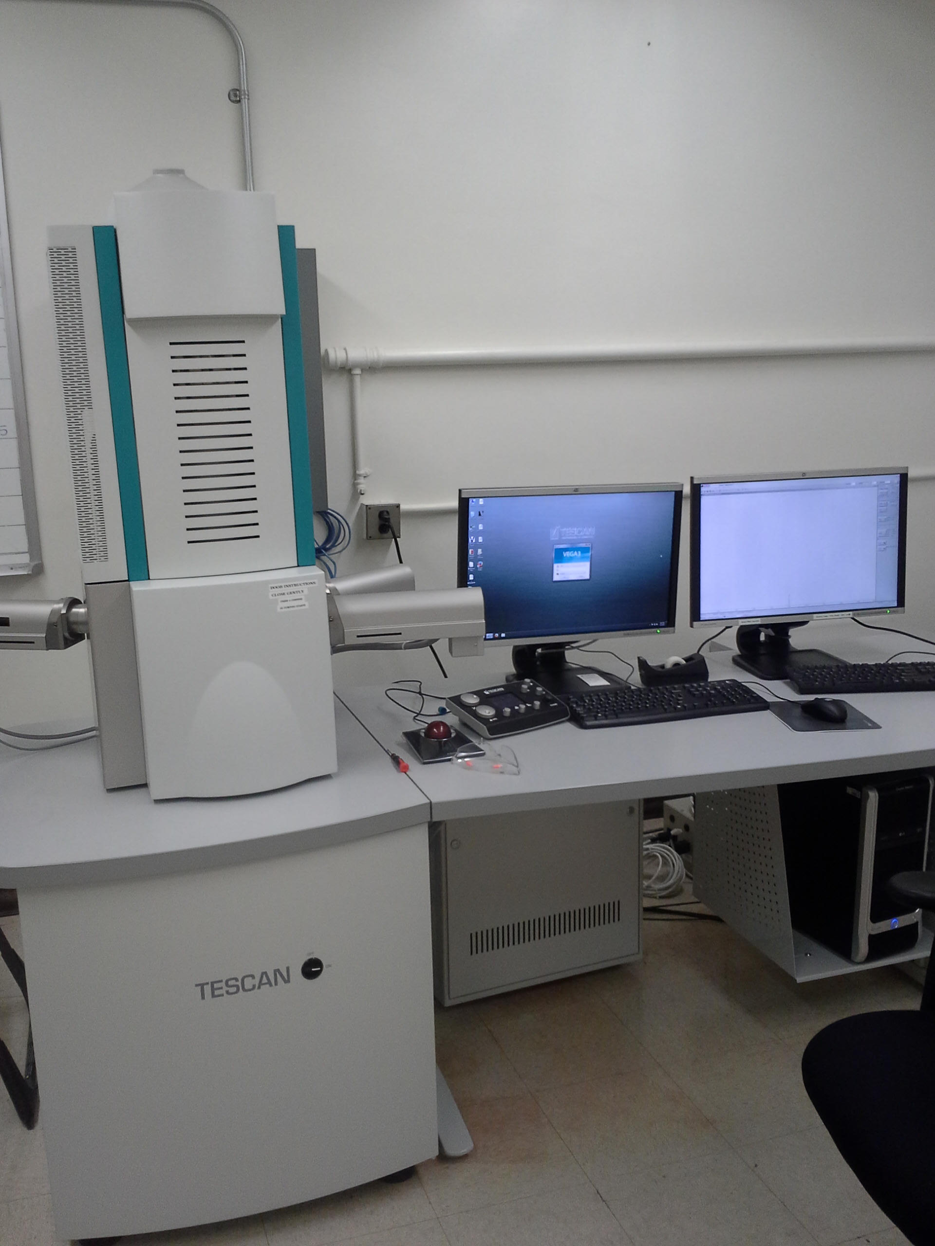
The SEM in our laboratory.
Scanning Electron Microscope
Capabilities
The Ion Microprobe Facility houses a Tescan Vega-3 XMU variable-pressure (VP)
Scanning Electron Microscope (SEM) for the imaging and analysis of solid
samples. Samples may be imaged
with several detectors including a secondary electron detector (SE) for
topographic imaging and backscattered electron (BSE) detector for
compositional variations, along with both panchromatic and 3-channel color
cathodoluminescence (CL) detectors.
The SEM is also equipped with an EDAX energy-dispersive x-ray
analysis (EDS) system for semi-quantitative sample compositional analysis
and elemental mapping.
The sample chamber will accommodate thin sections,
thick sections, ion probe mounts, pin mounts, and larger samples up to
several centimeters. Samples
are generally run with a conductive coating (either graphite or gold), but
BSE, EDS, and CL are also available for uncoated samples in low-vacuum mode.
Availability
The SEM was funded by a grant from the Army Research Office's Defense University Research Instrumentation Program (DURIP) with support for the CL detectors through the UCLA Shared Resources Consortium. It is available for use by all facility visitors, as well as UCLA researchers and students, after training through facility personnel.
Analysis modes
Secondary Electrons:

A secondary electron image of a bee's eye. Image courtesy Rita Economos (beekeeperess).
Backscattered Electrons:
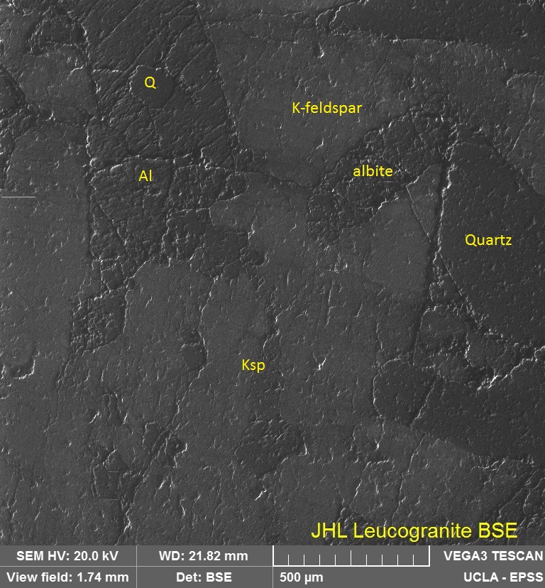
A backscattered electron image taken on our SEM of a leucogranite thin section.
Cathodoluminescence (color and panchromatic):
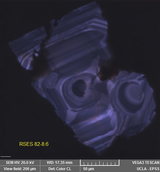
A color cathodoluminescence image taken on our SEM of a zircon crystal showing internal zonation.
Further information about Scanning Electron Microscopy:
- SEM introduction at Michigan State University
- SEM tutorial at Iowa State University
- UC Berkeley electron microscopy lab
- NAU course on Microbeam Techniques in Geology